Four synchronized DDS channels @500 MSPS
Independent frequency / phase / amplitude
control between all channels
Matched latencies for Freq, Phase, and Amplitude changes
Excellent channel to channel isolation
Frequency sweeping capability
Up to 16 levels of modulation (pin selectable)
Individually programmable DAC full scale currents
Four integrated 10-bit D/A converters(DACs)
32-bit frequency tuning resolution
14-bit phase offset resolution
10-bit output amplitude scaling resolution
Serial I/O Port(SPI) with enhanced data throughput
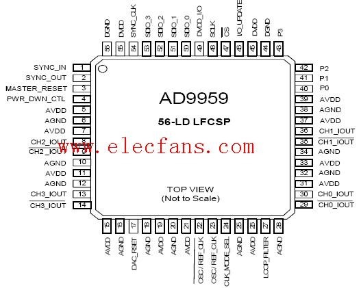
Pin Function Descriptions
Pin No. Mnemonic I/O Description
1 SYNC_IN I Used to synchronize multiple AD9959s. Connect to the SYNC_OUT pin of the master AD9959.
2 SYNC_OUT O Used to synchronize multiple AD9959s. Connect to the SYNC_IN pin of the slave AD9959.
3
MASTER_RESET
I Active high reset pin. Asserting the RESET pin forces the AD9959’s internal registers to their
default state, as described in the serial I/O port register map section in this document.
4 PWR_DWN_CTL I External Power-Down Control.
5,7,11,15,19,21,
26,31,33,37,39
AVDD I Analog Power Supply Pins (1.8V).
6,10,12,16,18,20,
25,28,32,34,38
AGND I Analog Ground Pins.
45, 55 DVDD I Digital Power Supply Pins (1.8 V).
44, 56 DGND I Digital Power Ground Pins.
8 CH2_IOUT O True DAC Output. Terminate into AVDD.
9
_________
CH2_IOUT
O Complementary DAC Output. Terminate into AVDD.
13 CH3_IOUT O True DAC Output. Terminate into AVDD.
14
_________
CH3_IOUT
O Complementary DAC Output. Terminate into AVDD.
17 DAC_RSET I Establishes the reference current for all DACs. A 1.962 kΩ resistor (nominal) is connected from
pin 17 to AGND.
22 OSC / REF_CLK I Complementary Reference Clock/Oscillator Input. When the REF_CLK is operated in singleended
mode, this pin should be decoupled to AVDD or AGND with a 0.1 μF capacitor.
23 OSC / REF_CLK I Reference Clock/Oscillator Input. When the REF_CLK is operated in single-ended mode, this is
the input.
24 CLK_MODE_SEL I Control Pin for the Oscillator Section. When high (1.8V), the oscillator section is enabled to
accept a crystal as the REFCLK source. When low, the oscillator section is bypassed.
CAUTION: Do not drive this pin beyond 1.8V.
27 LOOP_FILTER I Connect to the external zero compensation network of the PLL loop filter for the REFCLK
multiplier. For a 20x multiplier value the network should be a 1.2kΩ resistor in series with a 1.2
nF capacitor tied to AVDD.
29
_________
CH0_IOUT
O Complementary DAC Output. Terminate into AVDD.
30 CH0_IOUT O True DAC Output. Terminate into AVDD.
35
_________
CH1_IOUT
O Complementary DAC Output. Terminate into AVDD.
36 CH1_IOUT O True DAC Output. Terminate into AVDD.
40, 41,
42, 43
PS0, PS1,
PS2, PS3
I These Pins are synchronous to the SYNC_CLK (pin 54). Any change in Profile inputs transfers
the contents of the internal buffer memory to the I/O active registers (same as an external I/O
_UPDATE).
46 I/O_UPDATE I A rising edge detected on this pin transfers data from serial port buffer to active registers.
47 CS I Active low chip select allowing multiple devices to share a common I/O bus (SPI).
48 SCLK I Serial data clock for I/O operations. Data bits are written on rising edge of SCLK and read on
the falling edge of SCLK.
49 DVDD_I/O I 3.3 V Digital Power Supply for SPI port and I/O (excluding CLK_MODE_SEL).
50, 51
52, 53
SDIO_0, SDIO_1
SDIO_2, SDIO_3
I/O These data pins have multiple functions. Data I/O pins for the serial I/O port operation. They
are also used as data pins in modulation modes.
54 SYNC_CLK O I/O_UPDATE and Profile signals should meet the set-up and hold requirements with respect to
this signal in order to guarantee a fixed pipeline delay of data to DAC outputs.