Abstract: This article describes a vacuum fluorescent display (VFD) and some ideal applications for the technology. The reference design then shows how to use a MAX15005 power-supply controller in a flyback topology to obtain multiple output voltages for a vacuum fluorescent display.
Introduction
This reference design shows a solution for obtaining the drive voltage required for a vacuum fluorescent display (VFD) power supply in automotive applications. The design includes the complete schematic, and presents the bill of materials (BOM), load/line regulation measurements, and test results.
VFD Basics
The VFD is composed of three basic electrodes—the cathode filaments, anodes (phosphor), and grids—under a high-vacuum condition in a glass envelope. The cathode consists of fine tungsten wires, coated by alkaline earth metal oxides which emit electrons. The grids are a thin metal mesh, which controls and diffuses electrons emitted from the cathode. The anodes are conductive electrodes on which the phosphor is printed to indicate characters, icons, or symbols. Electrons emitted from the cathode are accelerated with positive potential applied to both grid and anode; upon collision with the anode the electrons excite the phosphor to emit light. The desired illuminated patterns can be achieved by controlling the positive or negative potentials on each grid and anode. The anode and grid require a DC-regulated voltage to avoid flickering of the display. For driving large VFDs, the cathode requires AC drive to prevent luminance slant, i.e., the difference in brightness from one side of the display to the other. A frequency range of 20kHz to 200kHz is recommended to avoid audible noise and flicker.
Design Specifications and Setup
This reference design features the MAX15005 power-supply controller optimized for automotive and VFD applications. The application circuit is designed to meet the following specifications:
VIN: 9V to 16V continuous, 5.5V to 40V transient
VANODE: 77VDC ±10% at 18mA (typ), 58mA (max)
VGRID: 55VDC ±10% at 14mA (typ), 41mA (max)
VFILAMENT: 3.1VAC ±10% at 350mA (typ), 385mA (max)
Output ripple: 77V: 1VP-P; 55V: 0.5VP-P
Line regulation, VIN = 9V to 16V:
VANODE = ±3%
VGRID = ±3%
VFILAMENT = ±5%
Load regulation: (see Line/Load Regulation Data section below)
Switching frequency: 22kHz
Temperature: -40°C to 125°C The schematic for the above specifications is shown in Figure 1. In this design MAX15005A is used in the flyback configuration for obtaining three output voltages.
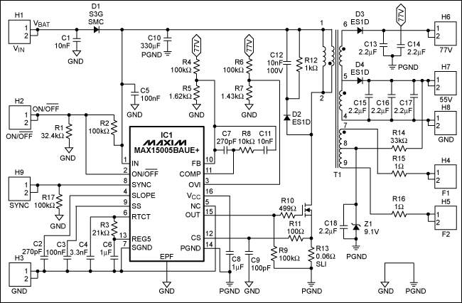
Figure 1. Schematic of the MAX15005B flyback converter for FSW = 22kHz.
The bill of materials (BOM) for this reference design is given in Table 1.
Table 1. Bill of Materials for VFD Reference Design
Designator
Value
Description
Part Number
Footprint
Manufacturer
Quantity
C1, C11, C12
10nF, 100V
Capacitor
C2012X7R2A103K
0805
TDK®
3
C2, C7
270pF, 100V
Capacitor
GRM188R72A271KA01D
0805
Murata®
2
C3, C5
100nF, 100V
Capacitor
C2012X7R2A104K
0805
TDK
2
C4
3.3nF, 25V
Capacitor
08053A332FAT2A
0805
AVX® Corporation
1
C6, C8
1µF, 50V
Capacitor
C3216X7R1H105K
1206
TDK
2
C9
100pF, 100V
Capacitor
GRM2165C2A101JA01D
0805
Murata
1
C10
330µF, 35V
Capacitor
–
SMD
TDK
1
C13, C14, C15, C16, C17, C18
2.2µF, 100V
Capacitor
GRM32ER72A225KA35L
1210
Murata
6
D1
3A, 400V
Diode
S3G
SMC
Vishay®
1
D2, D3, D4
1A, 200V
Diode
ES1D
SMA
Vishay
3
Q1
11A, 55V
n-FET
BUK92150-55A
–
NXP®
1
R1
32.4kΩ
Resistor
SMD, 5%, 0.125W
0805
KOA
1
R2, R9, R17
100kΩ
Resistor
SMD, 5%, 0.125W
0805
KOA
3
R3
21kΩ
Resistor
SMD, 1%, 0.125W
0805
KOA
1
R4, R6
100kΩ
Resistor
SMD, 1%, 0.250W
1206
KOA
2
R5
1.62kΩ
Resistor
SMD, 1%, 0.125W
0805
KOA
1
R7
1.43kΩ
Resistor
SMD, 1%, 0.125W
0805
KOA
1
R8
10kΩ
Resistor
SMD, 5%, 0.125W
0805
KOA
1
R10
499Ω
Resistor
SMD, 1%, 0.125W
0805
KOA
1
R11
100Ω
Resistor
SMD, 5%, 0.125W
0805
KOA
1
R12
1kΩ
Resistor
SMD, 1%, 0.333W
1210
KOA
1
R13
0.06Ω
Resistor
SMD, 1%, SL1
SL1
KOA
1
R14
33kΩ
Resistor
SMD, 5%, 0.125W
0805
KOA
1
R15, R16
1.0Ω
Resistor
SMD, 1%, 0.250W
1206
KOA
2
T1
54µH
Transformer
DCT20EFD-UxxSOA5
SMD
TDK
1
Z1
9.1V
Zener diode
1SMB5924BT
SMB
Vishay
1
IC1
MAX15005B
Boost controller
MAX15005BAUE+
16TSSOP
MAXIM®
1
Waveform Measurements
The following test results were generated from the board built for evaluating the circuit.
Test conditions: VIN = 14V; RANODE = 3.3kΩ; RGRID = 3.3kΩ; RFILAMENT = 8Ω.
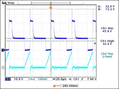
Ch1: MOSFET Q1 drain voltage (VDRAIN); Ch2: current-sense voltage across R13 (VISENSE).
Test conditions: VIN = 14V; RANODE = 3.3kΩ; RGRID = 3.3kΩ; RFILAMENT = 8Ω.
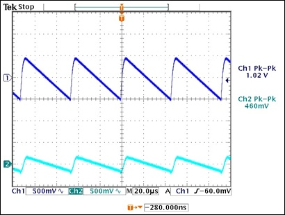
Ch1: anode output voltage ripple; Ch2: grid output voltage ripple.
Test conditions: VIN = 14V; RANODE = 3.3kΩ; RGRID = 3.3kΩ; RFILAMENT = 8Ω.
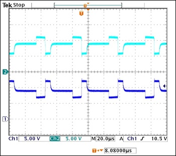
Ch1: filament positive node voltage (VF1); Ch2: filament negative node voltage (VF2).
Test conditions: VIN = 14V; RANODE = 3.3kΩ; RGRID = 3.3kΩ; RFILAMENT = 8Ω.
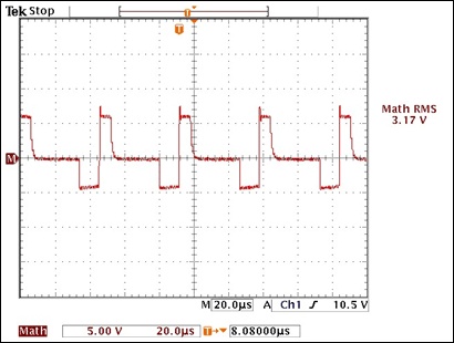
M: effective filament voltage (VF1 – VF2)
Line/Load Regulation Data
The following line/load regulation data was taken from the test board over the input voltage range and load.
VIN
I77 (mA)
I55 (mA)
V77 (VDC)
V55 (VDC)
VF (VRMS)
9.0
7.7
5.5
77.0
55.2
2.41
7.7
16.7
77.0
55.0
2.64
7.7
44.0
77.0
54.8
3.03
23.0
5.5
77.0
55.4
2.82
23.0
16.7
77.0
55.2
2.97
23.0
44.0
77.0
55.0
3.24
61.6
5.5
77.0
55.8
3.35
61.6
16.7
77.0
55.6
3.43
61.6
44.0
77.0
55.4
3.62
14.0
7.7
5.5
77.0
55.2
2.52
7.7
16.7
77.0
55.0
2.75
7.7
44.0
77.0
54.8
3.14
23.0
5.5
77.0
55.4
2.80
23.0
16.7
77.0
55.2
3.08
23.0
44.0
77.0
55.0
3.36
61.6
5.5
77.0
55.8
3.50
61.6
16.7
77.0
55.7
3.59
61.6
44.0
77.0
55.4
3.79
16.0
7.7
5.5
77.0
55.2
2.63
7.7
16.7
77.0
55.0
2.86
7.7
44.0
77.0
54.8
3.25
23.0
5.5
77.0
55.4
3.04
23.0
16.7
77.0
55.2
3.20
23.0
44.0
77.0
55.0
3.49
61.6
5.5
77.0
54.8
3.25
61.6
16.7
77.0
55.0
3.49
61.6
44.0
77.0
55.4
3.92
Conclusion
This application note presents a power-supply reference design for driving a typical vacuum fluorescent display in an automotive application. The design was built to the specifications presented here. The design was then tested. The circuit schematic, BOM, and typical waveforms have been presented.
AVX is a registered trademark of AVX Corporation.
Maxim is a registered trademark of Maxim Integrated Products, Inc.
Murata is a registered trademark of Murata Manufacturing Co., Ltd.
NXP is a registered trademark of NXP Semiconductors.
TDK is a registered trademark of TDK Corporation.
Vishay is a registered trademark of Vishay Intertechnology, Inc.